DipTrace 4.1.0.1 with 3D Libraries | 1.7 Gb
Languages: english & русский
Languages: english & русский
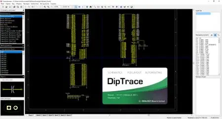
The Novarm software development team is pleased to announce the availability of DipTrace 4.1.0.1. The release 4.1 is brand new BOM generation and unparalleled Panelization features.
What's new in version 4.1
The focus of this release was to improve the design fluency and speed up your time to market. PCB Layout now features a brand new BOM generation tool with a variety of export options, including interactive HTML, and capacity to configure several Assembly Variants - a function that has also been added, among others, to the updated Pick and Place export. Moreover, all major Report tables are now auto updating (BOM, Pick and Place, Drill Size, Layer Stack). On top of that, our unparalleled Panelization tool makes creating of V-Scoring, Tab-Routing or combined panels really fast and easy.
On your requests, we’ve returned the import of raster images and refined 3D preview. Bulk substitution of patterns, which is now possible in Component Editor, will surely contribute to your design fluency.
You will also find a number of minor improvements, among which: optimization of trace editing, highlighting copper pours together with the nets they belong to for easier net integrity analysis in PCB, and alignment guidelines for texts and components as well as resizing of all panels by drag and drop in all modules.
A good deal of time has also been dedicated to expanding our libraries and enhancing IPC-7351 Pattern Generator, which now automatically creates 3D models for all families.
- Improved panelizing: V-Score and Tab Routing with mouse bites.
- Improved BOM, BOM in PCB Layout, Interactive BOM: integrated and HTML export.
- Improved Pick and Place: Center X/Y by component outline and terminals if exist, package height, updated dialog window.
- Assembly variants for BOM and Pick and Place.
- Improved Drill Size Report.
- Automatic update of report tables in PCB (BOM, Pick and Place, Drill Size, Layer Stack).
- Table rows and related components for report tables are highlighted.
- Raster pictures in PCB, improved raster pictures in Schematic.
- "Do not rotate marking with component" option.
- Improved trace editing: sharp angles are optimized, moving orthogonal trace with related 45 degree segments if necessary.
- Highlight copper pour islands and traces when highlight any trace or copper pour border.
- Align components and texts by other components and texts while moving.
- Resize of all panels (layers/properties/design manager, route, place component, etc) by mouse drag and drop.
- Bulk update of patterns in component libraries.
- Keep all pins of IPC-7351 3D model, not depending on pattern pads (option).
- Pattern description is displayed in Component Editor, Schematic and PCB.
- Basic part swap in Schematic.
- Remove ratline while deleting trace (option).
- 3D preview: Vector pictures in mask layer.
- Import/Export Improvements for DXF, Eagle, Altium ASCII, P-CAD ASCII.
- IPC-7351 Pattern Generator changes in CQFP, DFN 2 Pins, DFN 3 Pins, DFN 4 Pins, SOD, SODFL, Radial (Round LED), Radial (Rectangular LED), Radial (Disk), Radial (Disk, Offset Leads).
- IPC-7351 automatic 3D models for the following families:
Crystal(HC-49); Crystal; Chip Array, 2 Side Concave; Chip Array, 4 Side Concave;
Oscillator, Corner Concave; Oscillator, Side Concave;
Chip Array, 2 Side Flat; Chip Array, 4 Side Flat; LCC;
Chip, Side Concave(2, 4 Pins); Chip Array, 2 Side Convex;
DIP Socket; SIP; TO Cylindrical; Radial (Dipped, Round); Radial (Dipped, Rectangular); Radial (Dipped, Rectangular Offset Leads);
Radial (Disk); Radial (Disk, Offset Leads); Radial (Inductor); Radial (Molded).
- New libraries:
Con HDMI, Con Sockets DIP, Objects Fiducial, Objects Hardware Inch, Objects Hardware Metric,
Objects Jumper, Objects Lead Hole Pad, Objects Panelizing, Objects Testpoint, Objects Wire.
- Old libraries redesigned for IPC-7351:
Con Rect Headers, Con Rect Wire to Board, Con USB, Con Vacuum Tubes, Inductors, Potentiometers.
List of changes/fixes in DipTrace 4.1.0.1 if compared to 4.1.0.0
- Raster pictures from older versions are opened correctly in both Schematic and PCB(vectorizing is an option now).
- 4.1.0.1 files with raster pictures are now opened in 4.0 without crash. Pictures are notvisible as they are completely redesigned in 4.1, but other objects are ok.
- Cross-hair cursor option has been redesigned, it is also saved when you reopen theprogram.
- Converting component markings from 3.3 and earlier versions has been polished(lack of some markings was possible).
DipTrace is a PCB designing software that helps you design a neat and tidy board that works as per your needs. But when so many such software are available why should you choose to go with this specific tool?
Easier sub-section design. While designing a circuit, it is always comfortable to make small parts that you know would work for sure and then piece these together to form the complete circuit. But this is not as easy as it seems, as there are complications with making sure the signals flow correctly and with ensuring common ground connections.
You will find this problem easier to handle in DipTrace, where each sub-section can be designed on a separate sheet. The first sheet becomes the face of your design, to which the others can be linked hierarchically using connectors between sheets.
For nodes like power supplies or repeated ones in the design, you simply have to connect the nets to the same net port. The nets are then automatically linked across sheets, without wires. You can simply use a bus connection for groups of wires that go together. Nets on different sheets are connected by names, while buses on different sheets have exclusive connectors.
Once the schematic is complete, DipTrace allows you to cross-check parameters you might have missed, like shorts, or to super-impose pins by an electrical rule check (ERC) that is flexible in allowing you to choose the features you want to verify.
Pick and place your layout. Moving from the schematic design to the PCB layout stage, you can take forward the same schematic rules or import design rules from an earlier project. On importing non-schematic rules, your PCB is ready with net classes, layers and design constraints.
One of the major issues in creating layouts is the size: whether it will fit within the board it has to be printed on. This process is smooth with DipTrace, which lets you first draw a board outline in the required shape, manually pick and place whatever parts need to be fixed and then auto-place the rest. You can then add connections and fiddle around with your design to get the right component-connected layout.
Make the most of a customisable auto-router. Before you can begin routing your design, layers, via styles and net classes need your attention. These form the foundation of your board design, and with DipTrace you can customise and group your settings. The tool gives you the freedom to decide what signals should pass through which layer, choose colours, specify hole dimensions and manage via styles and net classes.
You can then decide how the auto-router should work, thus exercising complete control over your design, effortlessly. At any stage, you may save the settings in a rules file to use in a future project.
If you are going with the auto-router for routing your wires, there are grid based and advanced shape based options. You can set it up to work the way you want and it will automatically take care of your requirements.
If you choose to do it manually, you can select from available modes and, as you route, the tool warns you of design consistency errors. Thus, you take care of the design errors as you move along. You can always edit your work and even move nets between layers.
Remaining free spaces can use the copper-pour facility for low-impedance connections and additional heat-sinking. DipTrace allows you to organise different copper pours on a single layer, as well as connecting copper polygons on different layers into a single net.
A detailed procedure is available to verify the design. This includes checking for design rules and net connectivity. With errors shown at the exact location and different types marked in different colours, rectifying these becomes easy.
Relate the schematic and the layout. While completing your layout is important, it is as important to ensure that the schematic and the layout are in sync. There might be cases when you have to add components after the layout has been designed. With compare-to-schematic, renew-design-from-schematic and back-annotation features, this procedure is relatively simplified.
DipTrace Walkthrough
Established in 2002, Novarm is a software development company, specializing in state-of-the-art programs for PCB professionals and hobbyists, united into DipTrace design suite. We provide affordable, powerful and easy-to-use solution for electronic engineers worldwide. The software uses intuitive features and commands based on long-term heavy involvement into electronic designers community and observations how EDA software is actually used. We listen carefully to our customers telling us about their needs.
Product: DipTrace
Version: 4.1.0.1 with 3D Libraries
Supported Architectures: 32bit / 64bit
Website Home Page : https://diptrace.com/
Language: english, русский
System Requirements: PC *
Size: 1.7 Gb
Recommended System Requirements
- Windows XP / Vista / 7 / 8 / 8.1 / 10 (32, 64-bit)
- 1 GHz Pentium III processor or equivalent;
- 1 Gb RAM
- 2,0 Gb hard disk space;
- 1024x768 screen resolution or higher;
- OpenGL / DirectX 9.0 or higher.
- Windows XP / Vista / 7 / 8 / 8.1 / 10 (32, 64-bit)
- 1 GHz Pentium III processor or equivalent;
- 1 Gb RAM
- 2,0 Gb hard disk space;
- 1024x768 screen resolution or higher;
- OpenGL / DirectX 9.0 or higher.
Please visit my blog
Added by 3% of the overall size of the archive of information for the restoration
No mirrors please
Added by 3% of the overall size of the archive of information for the restoration
No mirrors please


