PCB Footprint Expert 23.13 | 37.2 mb
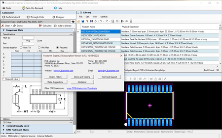
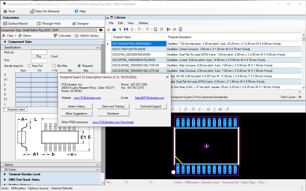
The software developer PCB Libraries, Inc is pleased to announce the availability of PCB Footprint Expert 23.13 Subscription Version (v.13 10/25/2023) . This solution lets you effortlessly calculate and generate high-quality footprints in a fraction of the time it would take you to create them using a CAD tool library editor.
Fixes & Enhancements:
Batch Build:
- Create new name in selected units not working
Options:
- "Rectangular End Cap" terminal definition changed to "Rectangular or Square End" per IPC-7352
- "Side Lead" definition changed to "Leadless" per IPC-7352
- J-Lead terminal option for Most Density Level toe changed from 0.01 to 0.10
- IPC-7352.opt – Changed Inward Flat Ribbon L Lead Height > 4.20 mm Least Density Side from -0.05 to 0.00
3D STEP:
- Chip and Molded body 3D polarity stripe can appear toward #2 pin in small package parts
FP Designer:
- Move Origin by X & Y using non-millimeter units isn’t working
- Assembly outline polarity not responding to Mirror or Rotate footprint commands
Library Editor:
- Code added to disallow extended ascii in all text either edited or pasted
Calculators:
- DFN 3 and 4 pin – The IPC footprint naming convention had the pin qty listed twice
- Corner Concave Package polarity dot is not following pad-silkscreen rule
Molded Body:
- Added Thyristor component family and 3D STEP model
- Added D – D1 nominal not to exceed 0.60 mm error flag
User Interface:
- Resize options now allowed on all dialog boxes
- Viewer mouse wheel functions re-defined – (no key) pan up/down, +shift - pan right left, +control - zoom in/out
CAD Tool Interfaces:
Altium:
- Added option to include footprint name in the ‘save-to’ directory path
KiCad:
- Pad non 0-90-180-270 orientations now allowed
- Rectangular thermal tab pattern defined solder mask shapes not filled
- Thermal tab rectangular shapes corners are always rounde
PCB Libraries is a culmination of decades of work, first started in 2003 with the bold vision of developing a “One World Standard PCB Footprint”. CAD library solutions developed by PCB Libraries has been used by over one hundred thousand PCB designers and engineers world-wide. The latest and greatest "PCB Footprint Expert" is designed to eliminate a vast amount duplication of effort wasted by - footprints and 3D models. PCB Libraries solutions streamline significant parts of the PCB design process with its CAD LEAP (Libraries Enhanced with Automated Preferences) technology, which supports 23 CAD formats with Footprints, 3D STEP models, and (soon) Schematic Symbols. The Library Expert can automatically create tens of millions of intelligent parts which can be batch-updated with dozens of user-defined settings (rotation, pad shapes, tolerance, line widths, etc). PCB Libraries is led by veteran technologists and provides enterprise-level library solutions to many household-name companies throughout the world.
PCB Footprint Expert Overview
This video is a high-level overview of how the PCB Footprint Expert can be used in combination with our "Parts on Demand" database to automatically generate high quality footprints and 3D models. This video was created using the Altium and 3D STEP outputs (each licensed separately).
PCB Libraries was started in 2003 as a sole proprietorship and was based on a couple of decades worth of work. The LP Wizard we developed over 12 years ago has for the most part remained unchanged after getting acquired in 2008 by Valor. Valor was later acquired by Mentor Graphics.
Owner: PCB Libraries, Inc.
Product Name: PCB Footprint Expert
Version: 23.13 Subscription Version (v.13 10/25/2023)
Supported Architectures: x86 or x64
Website Home Page : www.pcblibraries.com
Languages Supported: english
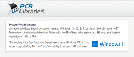
System Requirements: Windows *
Size: 37.2 mb
Please visit my blog
Added by 3% of the overall size of the archive of information for the restoration
No mirrors please
Added by 3% of the overall size of the archive of information for the restoration
No mirrors please


