Cmos Vlsi Design & Sub Systems Of Digital Circuits
MP4 | Video: h264, 1280x720 | Audio: AAC, 44.1 KHz
Language: English (US) | Size: 1.78 GB | Duration: 10h 54m
MP4 | Video: h264, 1280x720 | Audio: AAC, 44.1 KHz
Language: English (US) | Size: 1.78 GB | Duration: 10h 54m
Best VLSI Training Course for starting your career in VLSI Design& Subsystems of MOS circuits (schematic,stick,layouts)
What you'll learn
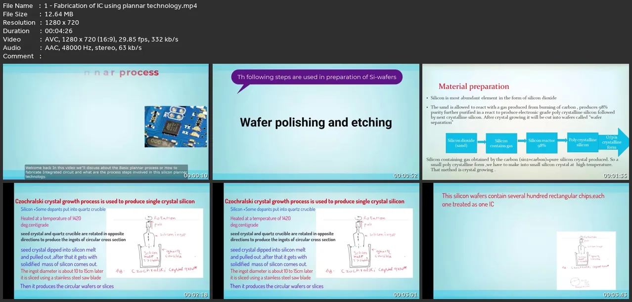
Basic Plannar Process or Fabrication process of an Integrated Chip
Basic Electrical Properties of MOS and BiCMOS Circuits
MOS & BiCMOS circuit design process (Including Stick and Layouts)
Basic circuits of NMOS, PMOS and CMOS circuits & Scaling of circuits
Subsystem design of digital circuits (includes combinational digital circuits)
Requirements
Having an interest on basic electronics but not needed the any expertise.
Description
Learn how to master on VLSI system Design & SubSystems of Digital Circuits and designing of different circuits like combinational and sequential etc. In this course you will learn very large scale integration design course from scratch and also covered each and every details with step by step procedure. Now a days very large scale integration technology emerging or growing day by day. You cannot imagine without the Basic VLSI Design & SubSystems of Digital Circuits or even electronics and integrated circuits because usage of electronic gadgets now becoming a part in our daily routines. So we much depend on VLSI system Design & SubSystems of Digital Circuits to design like portable electronic gadgets and other gadgets for different purposes. The silicon-integrated circuitry make it possible to design of digital circuits which may be very complex and most economical in space, power requirements and cost, and potentially very fast The area, power and cost have made silicon the dominant fabrication technology for electronics in very wide ranging areas of application. Like digital signal processing, analog and digital communications as well as in video processing etc. Metal oxide semiconductor (MOS) related circuitry will meet requirements but still it is being researched by ongoing improvements and the research in fabrication such that other techniques are being majorly adapted with gallium arsenide technology, including the use of materials other than silicon for the production of integrated circuits. . So its needed to learn VLSI system Design & SubSystems of Digital Circuits for better growth particularly for electronics and computer related people. So those who want to settle in VLSI design field learning these concepts is essential .so start your journey with this course from now onwards.In this course you may learn the behavior of MOS circuits in detail manner as well as you could get the better understanding after completion of this course.The course covers these topicsBasic Electrical Properties of metal oxide semiconductor(MOS) and Bipolar and metal oxide semiconductor circuitsCurrent and voltage relationship and its characteristicsThe Non-saturated regionSaturated regionMetal oxide semiconductor transistor transconductance and output conductance relationship.The pass transistorInverter characteristicsDetermination of pull up to pull down ration for an NMOS driven by another NMOS inverter.Pull up to pull down ratio for an NMOS Inverter driven by another NMOS inverter using the pass transistor.Complementary metal oxide semiconductor as inverter and its characteristics Transconductance and output conductanceAlternative forms of pull ups Bipolar and Complementary metal oxide semiconductor inverter circuits.MOS layers and NMOS color encoding with STICK AND mask layout schemesMOS layers and CMOS color encoding with STICK and mask layout schemesStick diagram rule setNmos inverter schematic and stick diagramNAND schematic and stick diagramsOperation of not nor or gatesStick diagram for NOR and OR gateCmos inverter schematic and stick diagramCMOS NAND schematic and stick diagramCMOS NAND twisted stick diagram and other modified models of sticks for NAND.CMOS NAND operation.CMOS NOR operation and stick diagramWhy design rules needed?lambda based layout rulesCMOS inverter and CMOS- NAND layoutsCMOS- NOR layoutSheet resistanceSheet resistance applied to Mos transistorsSheet resistance for depletion mode MOS inverterSheet resistance for CMOS inverterArea capacitance of layers and standard capacitance in different technologiesSome area capacitancesMultil layer area capacitanceTime delay in MOS circuitsInverter pair delay using NMOSCMOS inverter pair delayRise time estimation delayFall time estimation dealy and relation b/w rise and fall timeDriving of large capacitive loadsCascaded of inverter for N-even and odd conditionsCondition of pair delay to cascaded inverters for NMOSCondition of pair delay for CMOS cascaded inverterWhat is Super buffers ? Super buffers in inverting mode & non inverting modeWhat is scaling & Scaling for device parametersParity generator and its block diagram &Parity generator iin one-bit cellImplementation of Parity generator with Nmos and CMOS along with stick diagramWhat is Bus Arbitration logic and types of Bus arbitration logic?Bus arbitration logic ,truth table,logic expression,stick diagram, n-bit BALDesign of Multiplexers 2:1 and 4:1 with schematic and stick diagramDesign of 4 bit adder (Ripple carry adder)design of 4 bit adder (Ripple carry adder) Design of carry look ahead adder with CMOS schematic diagram-part2Feel free to ask any doubt while learning the courseHappy learning!Skill Gems EducationPUDI V V S NARAYANA
Who this course is for:
* Any one who want to learn more on VLSI DESIGN aspects in much more deeper its for you!,* Intermediate or engineering and post graduate or even company employees also can learn the course for better growth


